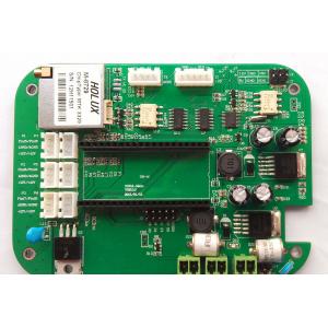
Turnkey Assembly PCBA Four Layer Board Lead Free Surface FinishingThickness 1.6mm FR4 Material One Stop PCB Solution
Product Description
Printed circuit board (pcb) and PCBA product areas
Communication terminals, communication stations, electronic communications, computers, household appliances, appliances, SD cards, SG cards, mobile phones, antennas, computers, automobiles, music equipment, playback equipment, banking equipment, medical instruments, medical equipment, medical equipment, aerospace, Aviation, military, LED, OLED, OLCD power control power supply, industrial power supply, communication power supply, automotive power supply, office equipment, digital products, computers and other product applications;
Winding circuit board (fpc) and FPCA product areas
CD, hard disk, printer, fax machine, scanner, sensor, mobile phone, connector, module, walkie-talkie antenna card, high-end camera, digital, camera, laser head, CD, medical, instrumentation, drive, automotive instrumentation, medical instrument , Medical equipment, banking equipment, industrial instruments, LED strips, military industry, aviation, aerospace, national defense and other high-tech products, more than 70% of the products are exported to the Americas, Europe, Japan, Asia Pacific and other countries and regions.
- Quality Assurance:
- Our Quality processes include:
- IQC: Incoming Quality Control (Incoming Materials Inspection)
- First Article Inspection for every process
- IPQC: In Process Quality Control
- QC: 100% Test & Inspection
- QA: Quality Assurance based on QC inspection again
- Workmanship: IPC-A-610, ESD
- Quality Management based on CQC, ISO9001:2008, ISO 14001:2004
- Certificates:
- ISO9001-2008
- ISO/TS16949
- UL
- IPC-A-600G and IPC-A-610E Class II compliance
- Customer's requirements
- Quick Detail:
- PCB Assembly on SMT and DIP
- PCB schematic drawing/ layout /producing
- PCBA clone/change board
- Components sourcing and purchasing for PCBA
- Enclosure design and plastic injection molding
- Full range of testing services. Including: AOI, Fuction Testing , In Circuit Testing, X-Ray For BGA Testing,
- aiC programming
- PCB, FPC product application field
Various digital products, automotive new energy, automotive products, military, aerospace, medical, wireless terminals, wired terminals, communication equipment, communication stations, finance, industrial industrial control, consumer electronics, educational equipment, smart devices, smart products, security, LED, computer, mobile phone and other electronic products
| PCBA | PCB+components sourcing+assembly+package |
| Assembly details | SMT and Thru-hole, ISO SMT and DIP lines |
| Lead Time | Prototype: 15 work days. Mass order: 20~25 work days |
| Testing on products | Flying Probe Test, X-ray Inspection, AOI Test, Functional test |
| Quantity | Min quantity: 1pcs. Prototype, small order, mass order, all OK |
| Files needed | PCB: Gerber files(CAM, PCB, PCBDOC) |
| Components: Bill of Materials(BOM list) |
| Assembly: Pick-N-Place file |
| PCB Panel Size | Min size: 0.25*0.25 inches(6*6mm) |
| Max size: 20*20 inches(500*500mm) |
| PCB Solder Type | Water Soluble Solder Paste, RoHS lead free |
| Components details | Passive Down to 0201 size |
| BGA and VFBGA |
| Leadless Chip Carriers/CSP |
| Double-sided SMT Assembly |
| Fine Pitch to 0.8mils |
| BGA Repair and Reball |
| Part Removal and Replacement |
| Component package | Cut Tape,Tube,Reels,Loose Parts |
PCB assembly
process | Drilling-----Exposure-----Plating-----Etaching & Stripping-----Punching-----Electrical Testing-----SMT-----Wave Soldering-----Assembling-----ICT-----Function Testing-----Temperature & Humidity Testing
|
FAQ:
Q: What files do you use in PCB fabrication?
A: Gerber or Eagle, BOM listing, X, Y sitting report, PNP and Components Position
Q: Is it possible you could offer sample?
A: Yes, we can custom you sample to test before mass production
Q: When will I get the quotation after sent Gerber, BOM and test procedure?
A: Within 6-48hours for PCB quotation and around 24-48 hours for PCBA quotation.
Q: According to the difficulty of high-layer boards, How can I know the process of my PCB production?
A: 7-35days for PCB production and components purchasing, and 14-20days for PCB assembly and Testing
Q: How can I make sure the quality of my PCB?
A: We ensure that each piece of PCB, PCBA pro