36-layer HDI4-stage blind buried VAI hole, ISOLA+FR-4+TG180,military products,HDI Printed Circuit Boards,hdi pcb
Product Description
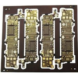
- Product structure: 36-layer HDI4-stage blind buried VAI hole, ISOLA+FR-4+TG180, high-frequency mixed pressure, laser hole 0.10mm, copper hole filling, inner and outer copper thickness 70um, hole copper 25um, impedance ±10%, board 4.5mm thick, Immersion gold 2u"
- Printed Circuit Boards are 94V0 compliant, and adhere to IPC610 Class 2 international PCB
- Standard.
- Quantities range from prototype to volume production.
- 100% E-Test
Printed circuit board (pcb) and PCBA product areas
Communication terminals, communication stations, electronic communications, computers, household appliances, appliances, SD cards, SG cards, mobile phones, antennas, computers, automobiles, music equipment, playback equipment, banking equipment, medical instruments, medical equipment, medical equipment, aerospace, Aviation, military, LED, OLED, OLCD power control power supply, industrial power supply, communication power supply, automotive power supply, office equipment, digital products, computers and other product applications; - Winding circuit board (fpc) and FPCA product areas
CD, hard disk, printer, fax machine, scanner, sensor, mobile phone, connector, module, walkie-talkie antenna card, high-end camera, digital, camera, laser head, CD, medical, instrumentation, drive, automotive instrumentation, medical instrument , Medical equipment, banking equipment, industrial instruments, LED strips, military industry, aviation, aerospace, national defense and other high-tech products, more than 70% of the products are exported to the Americas, Europe, Japan, Asia Pacific and other countries and regions.
PCB, FPC process production capability
| Technical ltem | MassProduct | Advanced Technology |
| 2016 | 2017 | 2018 |
| Max.Layer Count | 26L | 36L | 80L |
| Through-hole plate | 2~45L | 2~60L | 2~80L |
| Max.PCBSize(in) | 24*52" | 25*62" | 25*78.75" |
| The layer number of FPC | 1~36L | 1~50L | 1~60L |
| Max.PCBSize(in) | 9.8"*196" | 9.8"*196" | 10"*196"Reel to reel |
| Layeredplatelayer | 2~12L | 2~18L | 2~26L |
| Max.PCBSize(in) | 9"*48" | 9"*52" | 9"*62" |
| Combination of hard and soft layers | 3~26L | 3~30L | 3~50L |
| Interconnect HDI | 5+X+5Interconnect HDI | 7+X+7Interconnect HDI | 8+X+8,Interconnect HDI |
| HDI PCB | 4~45L | 4~60L | 4~80L |
| Interconnect HDI | 3+20+3 | 4+X+4Interconnect HDI | 4+X+4,Interconnect HDI |
| Max.PCBSize(in) | 24"*43" | 24"*49" | 25"*52" |
| Material | FR-4 Rogers | FR-4 Rogers | FR-4 Rogers |
| Base material | Halogenfree,LowDK | Halogenfree,LowDK | Halogenfree,LowDK |
| Build-up Material | FR-4 | FR-4 | FR-4 |
| BOard,Thickness(mm) | Min.12L(mm) | 0.43 | 0.42~8.0mm | 0.38~10.0mm |
| Min.16L(mm) | 0.53 | 1.60~8.0mm | 0.45~10.0mm |
| Min.18L(mm) | 0.63 | 2.0~8.0 | 0.51~10.0mm |
| Min.52L(mm) | 0.8 | 2.50~8.0mm | 0.65~10.0mm |
| MAX(mm) | 3.5 | 10.0mm | 10.0mm |
| Min.CoreThickness um(mil) | 254"(10.0) | 254"(10.0) | 0.10~254(10.0mm) |
| Min.Build up Dielectric | 38(1.5) | 32(1.3) | 25(1.0) |
| BaseCopperWeight | Inner Layer | 4/1-8 OZ | 4/1-15 OZ | 4/1-0.30mm |
| Out Layer | 4/1-10 OZ | 4/1-15 OZ | 4/1-30 OZ |
| Gold thick | 1~40u" | 1~60u" | 1~120u" |
| Nithick | 76~127u" | 76~200u" | 1~250u" |
| Min.HOle/Land um(mil) | 150/300(6/12) | 100/200(4/8) | 100/200(4/8) |
| Min.Laser via/landum(mil) | 60/170(2.4/6.8) | 50/150(2/6) | 50/150(2/6) |
| Min. IVH,Hole size/landum(mil) | 150/300(6/12) | 100/200(4/8) | 100/200(4/8) |
| DieletricThickness | 38(1.5) | 32(1.3) | 32(1.3) |
| 125(5) | 125(5) | 125(5) |
| SKipvia | Yes | Yes | Yes |
| viaoNhie(laserviaon BuriedPTH) | Yes | Yes | Yes |
| Laser Hole Filling | Yes | Yes | Yes |
| Technicalltem | Mass Product | Advanced Technolgy |
| 2017year | 2018year | 2019year |
| Drill hole depth ratio | ThroughHole | 2017year | .40:1 | .40:1 |
| Aspet Ratio | Micro Via | .35:1 | 1.2:1 | 1.2:1 |
| Copper Filling Dimple Size um(Mil) | 10(0.4) | 10(0.4) | 10(0.4) |
| Min.LineWidth&space | lnner Layer um(mil) | 45/45(1.8/1.8) | 38/38(1.5/1.5) | 38/38(1.5/1.5) |
| Plated Layer um(mil) | 45/45(1.8/1.8) | 38/38(1.5/1.5) | 38/38(1.5/1.5) |
| BGAPitch mm(Mil) | 0.3 | 0.3 | 0.3 |
| Min.PTH Hole ring um(mil) | 75(3mil) | 62.5(2.5mil) | 62.5(2.5mil) |
| Line Width Control | ∠2.5MIL | ±0.50 | ±0.50 | ±0.50 |
| 2.5Mil≤L/W∠4mil | ±0.50 | ±0.50 | ±0.50 |
| ≦3mil | ±0.60 | ±0.60 | ±0.60 |
| Laminated structure | Layer by layer | 3+N+3 | 4+N+4 | 5+N+5 |
| Sequential Build-up | 20L Any Layer | 36L Any Layer | 52L Any Layer |
| Multi-layer overlay | N+N | N+N | N+N |
| N+X+N | N+X+N | N+X+N |
| sequential Lamination | 2+(N+X+N)+2 | 2+(N+X+N)+2 | 2+(N+X+N)+2 |
| Soft and hard bonding | 2+(N+X+N)+2 | 2+(N+X+N)+2 | 2+(N+X+N)+2 |
| PTH filling process | PTH resin plug hole + plating fill
Electroplated hole/copper plug hole | PTH resin plug hole + plating fill
Electroplated hole/copper plug hole | PTH resin plug hole + plating fill
Electroplated hole/copper plug hole |
PCB, FPC main material supplier
| NO | supplier | Supply material name | Material origin |
| 1 | Japan | High frequency materials, PI, covering membrane,Copper berth | Mitsubishi Japan |
| 2 | dupont | High frequency materials, PI, covering film, dry film,Copper berth | Japan |
| 3 | panasonic | High frequency materials, PI, covering membrane,Copper berth | Japan |
| 4 | SanTie | PI, covering membrane | Japan |
| 5 | Born good | FR-4,PI,PP,Copper berth | shenzhen, China |
| 6 | A rainbow | PI, covering membrane,Copper berth | Taiwan |
| 7 | teflon | High frequency materials | The United States |
| 8 | Rogers | High frequency materials | The United States |
| 9 | Nippon Steel | PI, covering membrane,Copper berth | Taiwan |
| 10 | sanyo | PI, covering membrane,Copper berth | Japan |
| 11 | South Asia | FR-4,PI,PP,Copper berth | Taiwan |
| 12 | doosan | FR-4,PP | South Korea |
| 13 | Tai Yao plate | FR-4,PP,Copper berth | Taiwan |
| 14 | Alight | FR-4,PP,Copper berth | Taiwan |
| 15 | Yaoguang | FR-4,PP,Copper berth | Taiwan |
| 16 | Yalong | FR-4,PP | The United States |
| 17 | ISOAL | FR-4,PP | Japan |
| 18 | OAK | Buried, buried resistance, PP | Japan |
| 19 | United States 3M | FR-4,PP | The United States |
| 20 | Bergs | Copper and aluminum matrix | Japan |
| 21 | The sun | ink | Taiwan |
| 22 | Murata | ink | Japan |
| 23 | generous andbenevolent | PI, covering membrane,Copper berth | China's jiangxi |
| 24 | Yasen | PPI, covering membrane | China jiangsu |
| 25 | Yong Sheng Tai | ink | China guangdong panyu |
| 26 | mita | ink | Japan |
| 27 | Transcript | ceramic material | Taiwan |
| 28 | HOME | ceramic material | Japan |
| 29 | Fe-Ni-Mn | Alloy Invar, Section Steel | Taiwan |
| 30 | Yingtan | Copper and aluminum matrix | China's jiangxi |
Quality Assurance:
Our Quality processes include:
1. IQC: Incoming Quality Control (Incoming Materials Inspection)
2. First Article Inspection for every process
3. IPQC: In Process Quality Control
4. QC: 100% Test & Inspection
5. QA: Quality Assurance based on QC inspection again
6. Workmanship: IPC-A-610, ESD
7. Quality Management based on CQC, ISO9001:2008, ISO 14001:2004
Certificates:
ISO9001-2008
ISO/TS16949
UL
IPC-A-600G and IPC-A-610E Class II compliance
Customer's requirements
Quick Detail:
1. PCB Assembly on SMT and DIP
2. PCB schematic drawing/ layout /producing
3. PCBA clone/change board
4. Components sourcing and purchasing for PCBA
5. Enclosure design and plastic injection molding
6. Full range of testing services. Including: AOI, Fuction Testing , In Circuit Testing, X-Ray For BGA Testing,
7. IC programming
PCB, FPC product application field
Various digital products, automotive new energy, automotive products, military, aerospace, medical, wireless terminals, wired terminals, communication equipment, communication stations, finance, industrial industrial control, consumer electronics, educational equipment, smart devices, smart products, security, LED, computer, mobile phone and other electronic products
Surface treatment: full board OSP, full board immersion gold, whole board electric nickel gold, electric gold + immersion gold, electric gold + OSP, OSP + immersion gold, OSP + carbon bridge, gold finger, OSP + gold finger, immersion gold + gold finger, Shen tin, immersion silver, lead-free tin spray
FAQ:
Q: What files do you use in PCB fabrication?
A: Gerber or Eagle, BOM listing, X, Y sitting report, PNP and Components Position
Q: Is it possible you could offer sample?
A: Yes, we can custom you sample to test before mass production
Q: When will I get the quotation after sent Gerber, BOM and test procedure?
A: Within 6-48hours for PCB quotation and around 24-48 hours for PCBA quotation.
Q: According to the difficulty of high-layer boards, How can I know the process of my PCB production?
A: 7-35days for PCB production and components purchasing, and 14-20days for PCB assembly and Testing
Q: How can I make sure the quality of my PCB?
A: We ensure that each piece of PCB, PCBA products work well before shipping. We'll test all of them according to your test procedure.