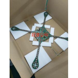
4L plate thicknesssize902*902mm,rigid flex printed +SMT+Plugin Drone product immersion goldpcb,High FrequencyPCB
Product Description
- 4L plate thicknesssize902*902mm,rigid flex printed +SMT+Plugin circuit boards PCB Board Service,4L plate thicknesssize902*902mm,rigid flex printed +SMT+Plugin Drone product,immersion gold pcb,Drone products, oversize
- Product area: Drone product
- Number of layers:
- 4L plate thickness: 1.0mm+SMT+Plugin+Electronic material purchasing
- Size: 902*902mm/1PCS
- Process structure:
- high frequency FR-4TG170+LSOLA, minimum hole 0.250mm,
- minimum line width 4/4mil Impedance Ω ± 10%
- Packing: vacuum packaging + moisture-proof beads + humidity card + wooden box or carton packaging
- Printed circuit board (pcb) and PCBA product areas
Communication terminals, communication stations, electronic communications, computers, household appliances, appliances, SD cards, SG cards, mobile phones, antennas, computers, automobiles, music equipment, playback equipment, banking equipment, medical instruments, medical equipment, medical equipment, aerospace, Aviation, military, LED, OLED, OLCD power control power supply, industrial power supply, communication power supply, automotive power supply, office equipment, digital products, computers and other product applications;
Winding circuit board (fpc) and FPCA product areas
CD, hard disk, printer, fax machine, scanner, sensor, mobile phone, connector, module, walkie-talkie antenna card, high-end camera, digital, camera, laser head, CD, medical, instrumentation, drive, automotive instrumentation, medical instrument , Medical equipment, banking equipment, industrial instruments, LED strips, military industry, aviation, aerospace, national defense and other high-tech products, more than 70% of the products are exported to the Americas, Europe, Japan, Asia Pacific and other countries and regions.
PCBA capabilities:
- Fast prototyping
- High mix, low and medium volume build
- SMT MinChip:0201
- BGA: 1.0 to 3.0 mm pitch
- Through-hole assembly
- Special processes (such as conformal coating and potting)
- ROHS capability
- IPC-A-610E and IPC/EIA-STD workmanship operation
PCB Assembly services:
- SMT Assembly
- Automatic Pick & Place
- Component Placement as Small as 0201
- Fine Pitch QEP - BGA
- Automatic Optical Inspection
PCB, FPC product application field
Various digital products, automotive new energy, automotive products, military, aerospace, medical, wireless terminals, wired terminals, communication equipment, communication stations, finance, industrial industrial control, consumer electronics, educational equipment, smart devices, smart products, security, LED, computer, mobile phone and other electronic products
Advantages:
1. Turnkey manufacturing or quick-turn prototypes
2. Board-level assembly or complete system integration
3. Low-volume or mixed-technology assembly for PCBA
4. Even consignment production
5. Supoorted capabilities
PCB, FPC process production capability
| Technical ltem | MassProduct | Advanced Technology |
| 2016 | 2017 | 2018 |
| Max.Layer Count | 26L | 36L | 80L |
| Through-hole plate | 2~45L | 2~60L | 2~80L |
| Max.PCBSize(in) | 24*52" | 25*62" | 25*78.75" |
| The layer number of FPC | 1~36L | 1~50L | 1~60L |
| Max.PCBSize(in) | 9.8"*196" | 9.8"*196" | 10"*196"Reel to reel |
| Layeredplatelayer | 2~12L | 2~18L | 2~26L |
| Max.PCBSize(in) | 9"*48" | 9"*52" | 9"*62" |
| Combination of hard and soft layers | 3~26L | 3~30L | 3~50L |
| Interconnect HDI | 5+X+5Interconnect HDI | 7+X+7Interconnect HDI | 8+X+8,Interconnect HDI |
| HDI PCB | 4~45L | 4~60L | 4~80L |
| Interconnect HDI | 3+20+3 | 4+X+4Interconnect HDI | 4+X+4,Interconnect HDI |
| Max.PCBSize(in) | 24"*43" | 24"*49" | 25"*52" |
| Material | FR-4 Rogers | FR-4 Rogers | FR-4 Rogers |
| Base material | Halogenfree,LowDK | Halogenfree,LowDK | Halogenfree,LowDK |
| Build-up Material | FR-4 | FR-4 | FR-4 |
| BOard,Thickness(mm) | Min.12L(mm) | 0.43 | 0.42~8.0mm | 0.38~10.0mm |
| Min.16L(mm) | 0.53 | 1.60~8.0mm | 0.45~10.0mm |
| Min.18L(mm) | 0.63 | 2.0~8.0 | 0.51~10.0mm |
| Min.52L(mm) | 0.8 | 2.50~8.0mm | 0.65~10.0mm |
| MAX(mm) | 3.5 | 10.0mm | 10.0mm |
| Min.CoreThickness um(mil) | 254"(10.0) | 254"(10.0) | 0.10~254(10.0mm) |
| Min.Build up Dielectric | 38(1.5) | 32(1.3) | 25(1.0) |
| BaseCopperWeight | Inner Layer | 4/1-8 OZ | 4/1-15 OZ | 4/1-0.30mm |
| Out Layer | 4/1-10 OZ | 4/1-15 OZ | 4/1-30 OZ |
| Gold thick | 1~40u" | 1~60u" | 1~120u" |
| Nithick | 76~127u" | 76~200u" | 1~250u" |
| Min.HOle/Land um(mil) | 150/300(6/12) | 100/200(4/8) | 100/200(4/8) |
| Min.Laser via/landum(mil) | 60/170(2.4/6.8) | 50/150(2/6) | 50/150(2/6) |
| Min. IVH,Hole size/landum(mil) | 150/300(6/12) | 100/200(4/8) | 100/200(4/8) |
| DieletricThickness | 38(1.5) | 32(1.3) | 32(1.3) |
| 125(5) | 125(5) | 125(5) |
| SKipvia | Yes | Yes | Yes |
| viaoNhie(laserviaon BuriedPTH) | Yes | Yes | Yes |
| Laser Hole Filling | Yes | Yes | Yes |
| Technicalltem | Mass Product | Advanced Technolgy |
| 2017year | 2018year | 2019year |
| Drill hole depth ratio | ThroughHole | 2017year | .40:1 | .40:1 |
| Aspet Ratio | Micro Via | .35:1 | 1.2:1 | 1.2:1 |
| Copper Filling Dimple Size um(Mil) | 10(0.4) | 10(0.4) | 10(0.4) |
| Min.LineWidth&space | lnner Layer um(mil) | 45/45(1.8/1.8) | 38/38(1.5/1.5) | 38/38(1.5/1.5) |
| Plated Layer um(mil) | 45/45(1.8/1.8) | 38/38(1.5/1.5) | 38/38(1.5/1.5) |
| BGAPitch mm(Mil) | 0.3 | 0.3 | 0.3 |
| Min.PTH Hole ring um(mil) | 75(3mil) | 62.5(2.5mil) | 62.5(2.5mil) |
| Line Width Control | ∠2.5MIL | ±0.50 | ±0.50 | ±0.50 |
| 2.5Mil≤L/W∠4mil | ±0.50 | ±0.50 | ±0.50 |
| ≦3mil | ±0.60 | ±0.60 | ±0.60 |
| Laminated structure | Layer by layer | 3+N+3 | 4+N+4 | 5+N+5 |
| Sequential Build-up | 20L Any Layer | 36L Any Layer | 52L Any Layer |
| Multi-layer overlay | N+N | N+N | N+N |
| N+X+N | N+X+N | N+X+N |
| sequential Lamination | 2+(N+X+N)+2 | 2+(N+X+N)+2 | 2+(N+X+N)+2 |
| Soft and hard bonding | 2+(N+X+N)+2 | 2+(N+X+N)+2 | 2+(N+X+N)+2 |
| PTH filling process | PTH resin plug hole + plating fill
Electroplated hole/copper plug hole | PTH resin plug hole + plating fill
Electroplated hole/copper plug hole | PTH resin plug hole + plating fill
Electroplated hole/copper plug hole |
Complete box build
Complete 'Box Build' solutions including materials management of all components, electromechanical parts,
plastics, casings and print & packaging material
Testing Methods
AOI Testing
Checks for solder paste
Checks for components down to 0201"
Checks for missing components, offset, incorrect parts, polarity
X-Ray Inspection
X-Ray provides high-resolution inspection of:
BGAs
Bare boards
In-Circuit Testing
In-Circuit Testing is commonly used in conjunction with AOI minimizing functional defects caused by
component problems.
Power-up Test
Advanced Function Test
Flash Device Programming
Functional testing
Quality Processes:
1. IQC: Incoming Quality Control (Incoming Materials Inspection)
2. First Article Inspection (FAI) for every process
3. IPQC: In Process Quality Control
4. QC: 100% Test & Inspection
5. QA: Quality Assurance based on QC inspection again
6. Workmanship: IPC-A-610, ESD
7. Quality Management based on CQC, ISO9001:2008, ISO/TS16949
Design file format:
1. Gerber RS-274X, 274D, Eagle and AutoCAD's DXF, DWG
2. BOM (bill of materials)
3. Pick and place file (XYRS)
FAQ:
Q: What files do you use in PCB fabrication?
A: Gerber or Eagle, BOM listing, X, Y sitting report, PNP and Components Position
Q: Is it possible you could offer sample?
A: Yes, we can custom you sample to test before mass production
Q: When will I get the quotation after sent Gerber, BOM and test procedure?
A: Within 6-48hours for PCB quotation and around 24-48 hours for PCBA quotation.
Q: According to the difficulty of high-layer boards, How can I know the process of my PCB production?
A: 7-35days for PCB production and components purchasing, and 14-20days for PCB assembly and Testing
Q: How can I make sure the quality of my PCB?
A: We ensure that each piece of PCB, PCBA products work well before shipping. We'll test all of them according to your test procedure.